
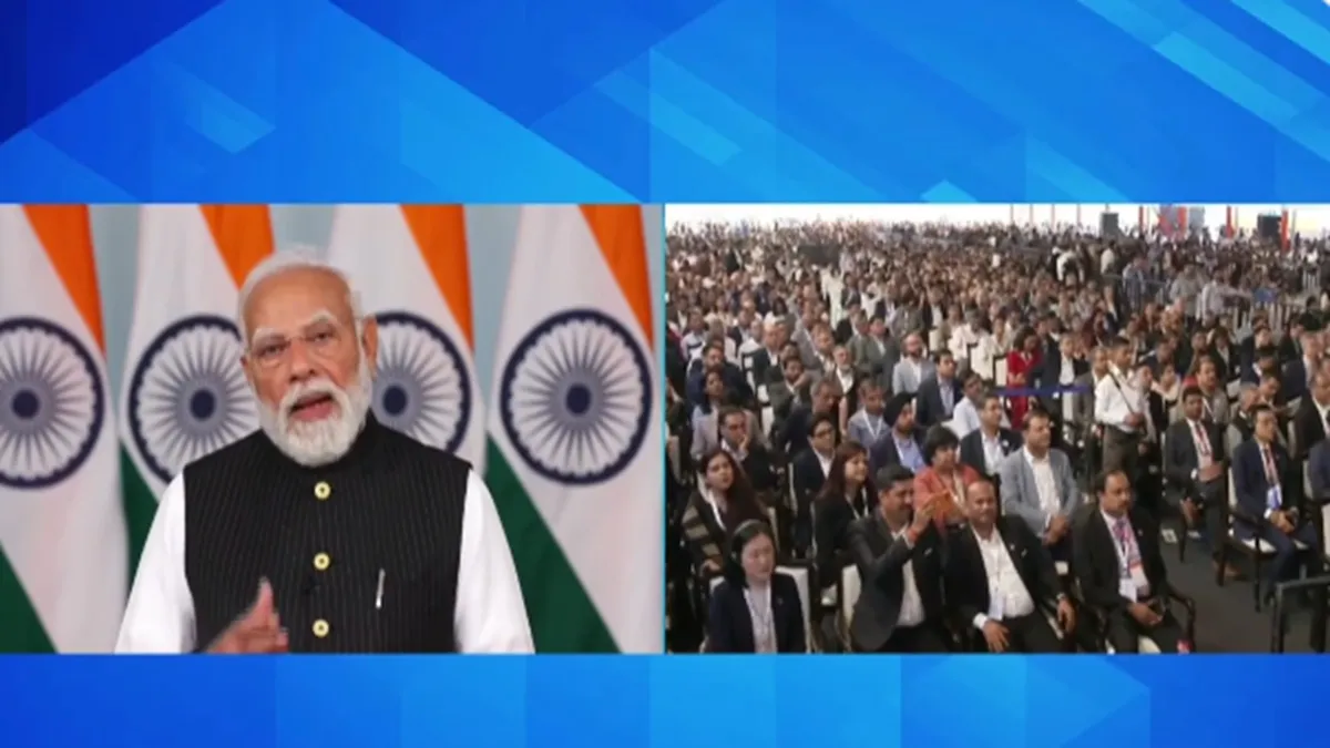
Prime Minister Narendra Modi inaugurated the HCL-Foxconn joint venture project, India Chip Pvt Ltd, via video conferencing from the Yamuna Expressway Industrial Development Authority (YEIDA) site in Uttar Pradesh. He hailed Uttar Pradesh's emergence as a pivotal hub in India's burgeoning semiconductor ecosystem, stressing the nation's drive toward chip production independence. This Outsourced Semiconductor Assembly and Test (OSAT) facility, backed by over Rs 3,700 crore investment, targets display driver chips for mobiles, laptops, autos, and consumer electronics.
Vision for a 'Tech-ade' and rapid progress
Modi declared this decade India's "tech-ade," with semiconductor investments laying the groundwork for 21st-century dominance. Despite a late start, India has greenlit 10 such units under its Semiconductor Mission, four nearing production. He linked the launch to the freshly concluded India AI Impact Summit in Delhi, where global leaders applauded India's tech vision, and noted 2026's blistering pace since January, calling this week historic.
Strategic boost to manufacturing and jobs
The YEIDA plant, under the Modified ATMP scheme, will process 20,000 wafers monthly, slashing import reliance and fortifying supply chains for key sectors. It promises thousands of direct and indirect jobs for engineers and technicians, sparking ancillary growth, startups, design hubs and skill upgrades. Proximity to Jewar Airport enhances logistics, cementing UP's role in global electronics while advancing Atmanirbhar Bharat.
Global partnerships fuel national ambition
HCL's hardware prowess merges with Foxconn's manufacturing might, marking the sixth mission-approved unit and UP's first. Modi emphasised how such facilities ignite innovation ecosystems wherever established. This step aligns with unprecedented tech outlays shaping humanity's future, positioning India as a reliable high-end electronics partner worldwide.